
 MTCN(003026)
Production
01

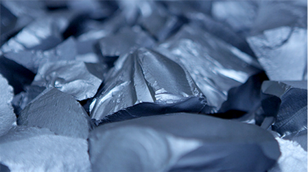
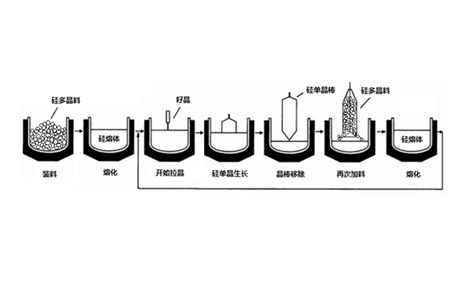
Preparing materials
Prepare a certain amount, proportion of polysilicon and dopant into single crystal quartz crucible furnace.
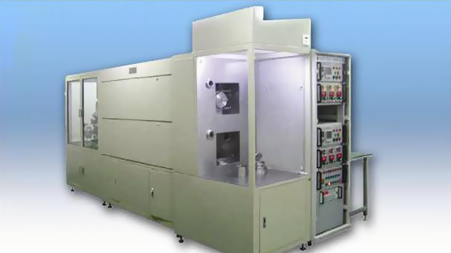
02

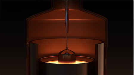
Crystal growth
By making use of the single crystal furnace semiconductor grade polysilicon at the highest thermal field in the melting temperature of 1500 ℃, and then through the crystal growth "pulled the diameter according to user's requirements
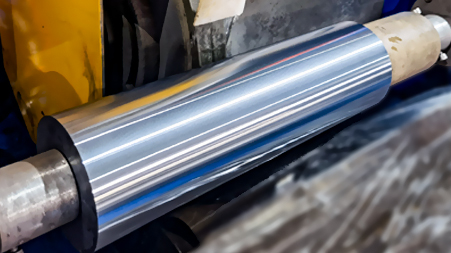
03

Rounded
The growth of single crystal ingot after external circular grinding diamond wheel, made of silicon rod after grinding has the standard of the diameter of the cylinder.
06

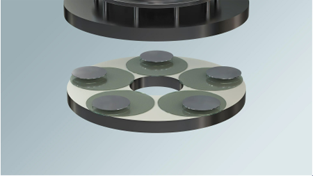
Grinding
The use of star wheel will be placed in the silicon wafer double grinder between the upper and lower disc, adding liquid abrasive material, make the silicon wafer with the disc for relative planetary movement, and the silicon wafer section pressure double grinding processing, improve the thickness tolerance between the wafer and wafer wafer flatness and parallelism.
05

Chamfering
The edge profile of the chip was grinded by diamond grinding wheel to reduce the fragmentation in subsequent silicon wafer processing and device process.
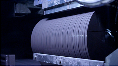
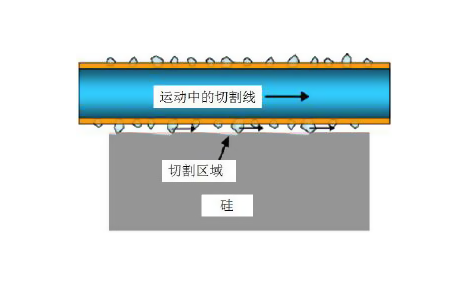
04

Slice
After rolling process of silicon rods, cut into a certain thickness of the silicon wafer.
07

Polishing
Using polishing liquid on the surface of silicon wafer mechanical polishing and chemical etching of the dual role for unprocessed damage level (mirror) smooth silicon wafer surface.
08

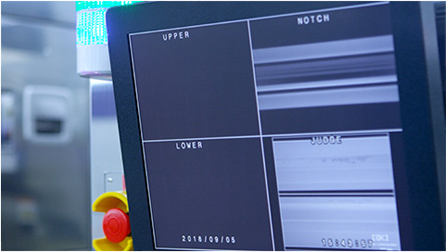
Inspection
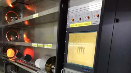
According to the requirements of silicon product standards implement inspection.
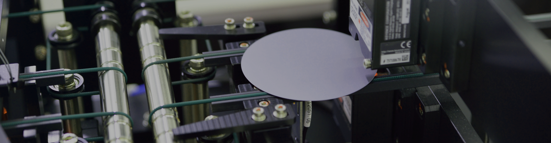
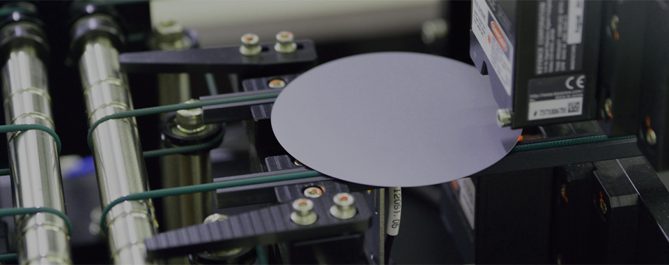
09

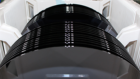
Polished wafer
All kinds of specifications of high quality monocrystalline silicon slice.
12
LTO film edge stripping
The oxide film edge stripping machine is used to strip the oxide film produced by APCVD process at the edge of silicon wafer, so as to eliminate the influence of oxide film at the edge of silicon wafer on epitaxial process.
11

LPVCD
LPCVD furnace is used to deposit intrinsic polycrystalline silicon (I-poly) on the back of silicon wafer, and the polycrystalline silicon film plays the role of absorbing metal ions in silicon wafer. For enhanced external impurity absorption process.
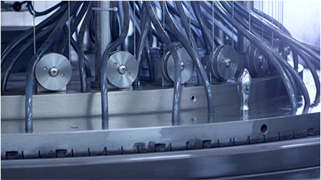
10

APCVD
APCVD furnace is used to deposit low-temperature oxide film (LTO) on the back of silicon wafer to prevent dopant inside silicon wafer from spilling and diffusing into the epitaxial layer on the front of silicon wafer during silicon wafer epitaxy process.
Core Technology
Feeding again draw technology
Multiple feeding, improve equipment efficiency and utilization of crucible, increase the rate of doping on file.
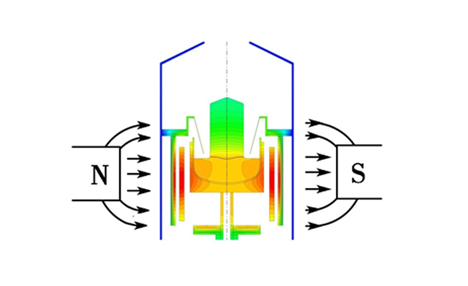
Magnetic field pulling of monocrystalline silicon technology
Can realize low oxygen content, low lattice defect density, radial doped czochralski single crystal homogeneous products.
Semiconductor single crystal king kong line line
Kong line wire cutting technology, compared to the traditional mortar cut, cutting speed faster, less monolithic materials, monolithic cheaper, and more slice thickness